From June 3rd to 5th, we cordially invite you to join us at E3-D38 at the 2026 Shanghai International Semiconductor Technology Conference and Exhibition!
As cutting-edge technologies such as artificial intelligence, smart cars, and 5G communication sweep across the globe, the semiconductor industry has become the core engine driving a new round of technological revolution and industrial transformation. As the core hub of the global electronic manufacturing industry and the largest semiconductor consumer market, China’s semiconductor industry has entered a stage of rapid development driven by both policy dividends and market demand. The 14th Five Year Plan clarifies the direction of industrial layout, and Shanghai is guided by the “20+8” industrial policy to fully build the third pole of the national semiconductor industry. The forefront fields such as third-generation semiconductors have ushered in a strategic window period of explosive growth.

At this critical juncture of industrial development, the 2026 Shanghai International Semiconductor Technology Conference and Exhibition will be held from June 3-5, 2026 at the Shanghai New International Expo Center. This exhibition is expected to have an exhibition area of 60000 square meters, gathering more than 1000 industry-leading exhibitors and attracting over 100000 professional visitors. It is a top-level professional platform for technology exchange, resource docking, and win-win cooperation in the entire semiconductor industry chain. As an innovative enterprise deeply rooted in the field of semiconductor materials, Shanghai Paralon New Materials Co., Ltd. has always focused on the core pain points of the semiconductor industry, with the mission of “empowering the future of technology with material innovation”. It continues to deepen its cultivation in the field of semiconductor special coating protection and functional coating, providing professional and reliable technical support and customized solutions for the entire process of chip design, manufacturing, packaging and testing. We cordially invite you to visitE3-D38At the booth, we will focus on showcasing the innovative achievements of our three core business lines:
Parylene coating

With the characteristics of no pinholes, corrosion resistance, and excellent insulation performance, it can provide comprehensive and multi-dimensional protection for semiconductor devices, effectively improving the stability and service life of chips in complex working environments. It is widely used in the protection scenarios of high-end electronic devices such as high-end chips and precision sensors.
UV (UV curable) coating

Fast curing speed and strong adhesion enable rapid modification and functional upgrading of semiconductor device surfaces, meeting the stringent requirements for efficient and precise coating processes in fields such as 5G communication and consumer electronics, and helping products achieve technological breakthroughs in miniaturization and lightweighting.
ALD (Atomic Layer Deposition) coating
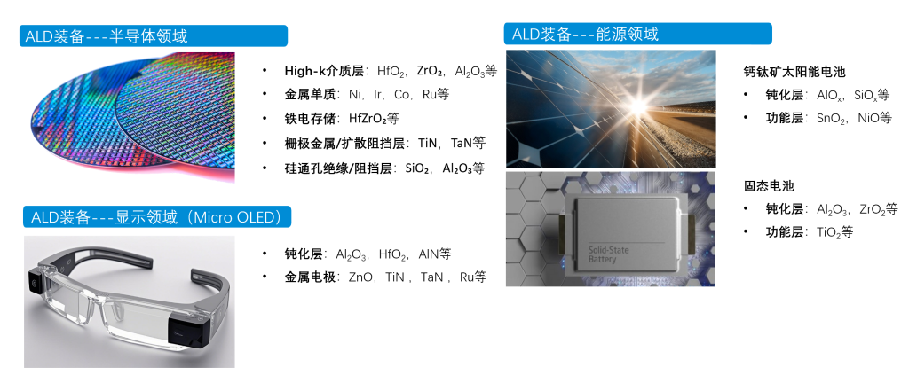
It can achieve atomic level precision in thin film deposition, provide ultra-thin and uniform functional coatings for semiconductor devices, accurately control the electrical and optical properties of devices, and demonstrate broad application prospects and technological value in cutting-edge fields such as third-generation semiconductors and advanced packaging. During the exhibition, we had in-depth exchanges with industry experts and business partners on cutting-edge technologies of semiconductor coating materials, jointly exploring industry development trends, technological application innovation, and win-win cooperation paths. Whether you are an upstream and downstream enterprise in the semiconductor industry chain or a technical practitioner who pays attention to industry development, we will provide you with high-quality opportunities for in-depth communication and resource docking. Shanghai Paralon New Materials Co., Ltd. looks forward to meeting you at the Shanghai New International Expo Center to explore the infinite possibilities of the semiconductor industry and work together to create a new technological future!