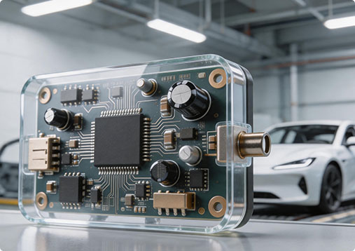
Product Overview
Atomic layer deposition (ALD) is based on self limiting surface reactions and can achieve uniform thin film deposition with Emmy level accuracy on complex structures.
core strengths
- Deposition accuracy<1 nm, step coverage>95%
- Layer by layer sedimentation, precise and controllable thickness
- Low temperature process, suitable for sensitive substrates
- Ideal choice for chip level protection of semiconductors, lithium batteries, photovoltaics, and other materials
Scope of application
ALD Equipment – Semiconductor Field
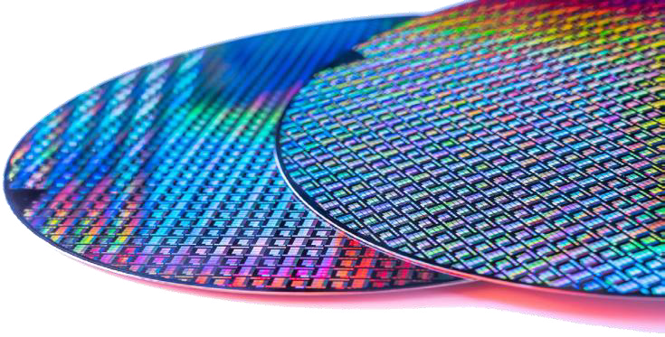
High-k dielectric layer: HfO2, ZrO ₂, Al2O3, etc
• Metallic elements: Ni, Ir, Co, Ru, etc
• Ferroelectric storage: HfZrO ₂, etc
• Gate metal/diffusion barrier layer: TiN, TaN, etc
• Through silicon via insulation/barrier layer: SiO ₂, Al ₂ O3, etc
ALD Equipment – Display Field (Micro OLED)
Passivation layer: Al2O3, HfO2, AlN, etc
• Metal electrodes: ZnO, TiN, TaN, Ru, etc
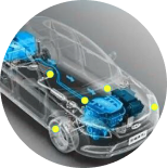
ALD Equipment – Energy Sector

Perovskite solar cells
Passivation layer: AlOx, SiOx, etc
• Functional layer: SnO2, NiO, etc
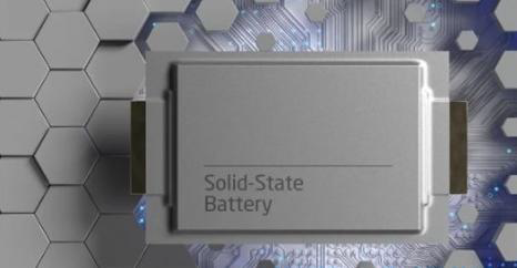
solid-state battery
Passivation layer: Al2O3, ZrO2, etc
• Functional layer: TiO2, etc
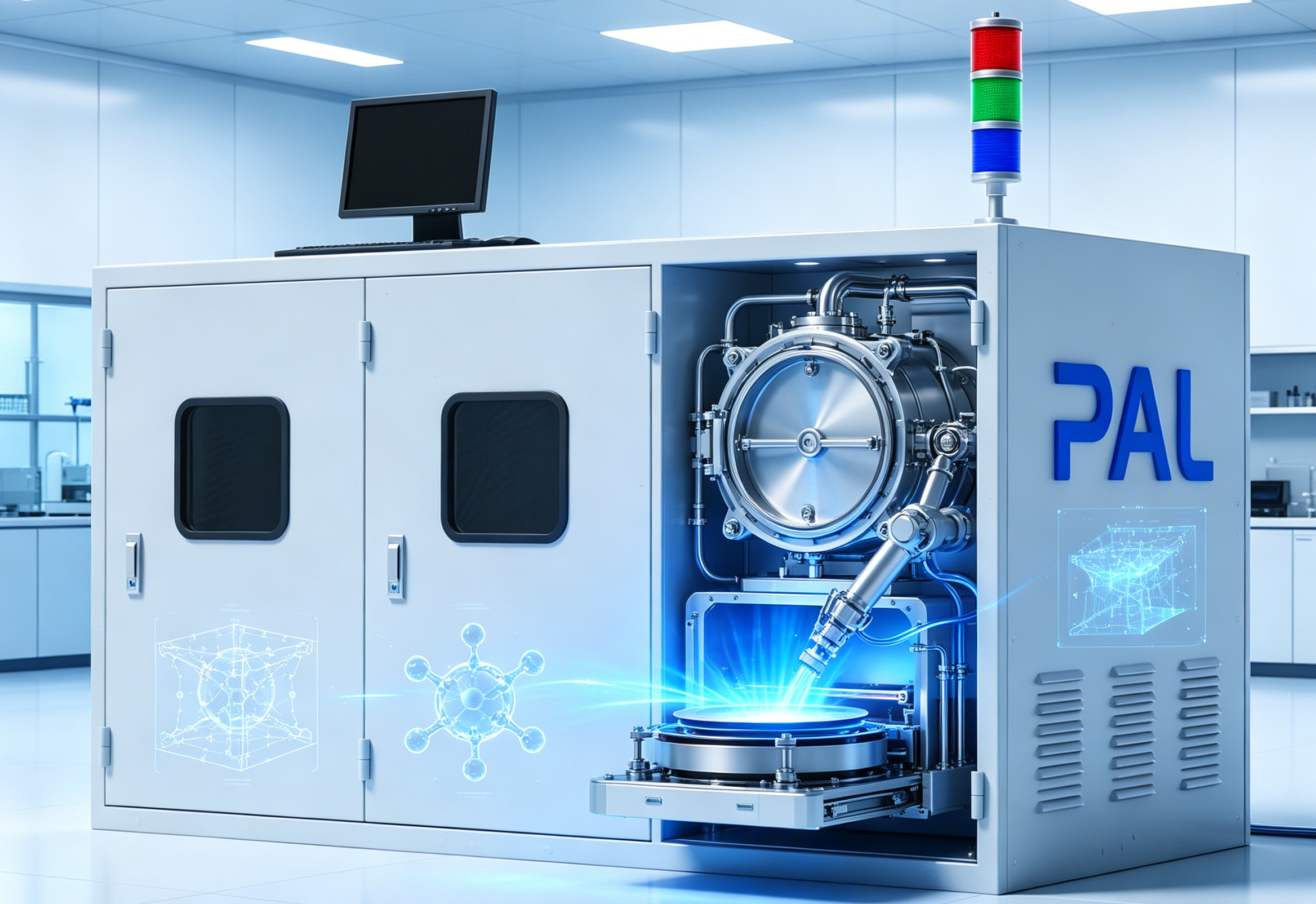
Paralon ALD equipment customization
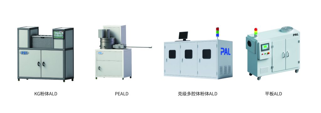
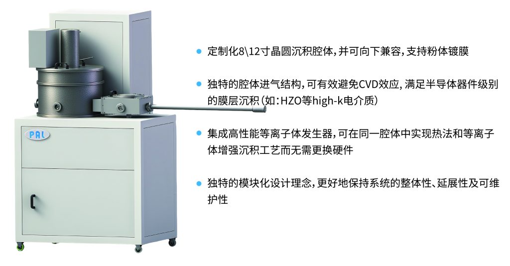
Paralon | Flat ALD products
The Paralon A-100 is an ALD platform specifically designed for scientific research and enterprise development. Every detail of the device is fully considered to be multifunctional, modular, and user-friendly. For Paralon, it is very important to allow users to freely develop processes and various applications without being limited by equipment. The A-100 represents the most advanced design concept and atomic layer thin film deposition solution, which enables the preparation of high-quality semiconductor grade thin films on various sizes and substrate materials.
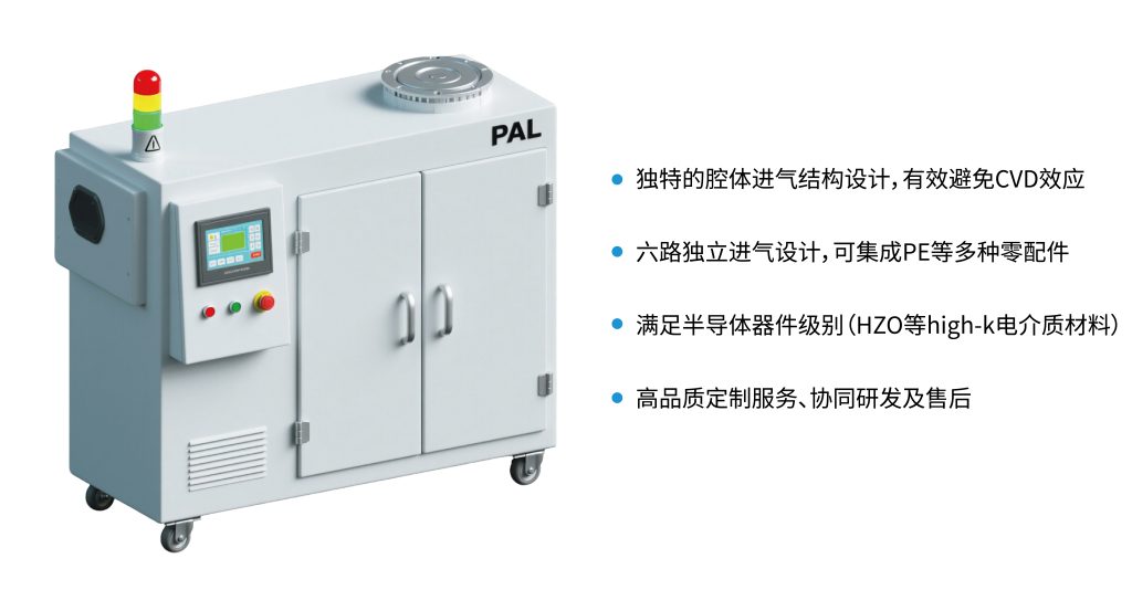
Pelalon | PEALD products
The PAL-D series machines belong to the time type ALD deposition equipment of Shanghai Paralon New Materials Co., Ltd. The PAL-D series is mainly aimed at universities, research institutes, and enterprise R&D teams, allowing users to freely develop various processes and materials. Currently, good data has been obtained in the actual deposition process of oxide (such as Al2O3, HfO2, ZrO2, HZO, etc.) and nitride (TiN, AlN, etc.) thin films, which is suitable for various semiconductor device functional layers, insulation layers, passivation layers, and other fields of thin film deposition needs.
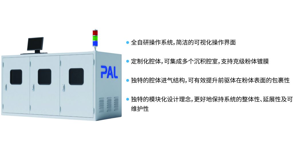
Paralon | Gram grade Powder ALD Products
PAL-P series machines are ALD coating equipment specially developed by Shanghai Paralon New Materials Co., Ltd. for powder samples. The P series is mainly aimed at universities, research institutes, and enterprise R&D teams, suitable for surface modification of various catalysts, battery electrode coatings, medical powder formulations, etc. Generally, sedimentary materials are mainly thin films of oxides (such as Al2O3, TiO2, etc.) and nitrides (TiN, etc.).
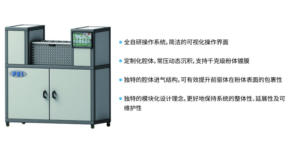
Paralon | Kilogram sized Powder ALD Products
PAL-P series machines are ALD equipment specially launched by Shanghai Paralon New Materials Co., Ltd. for the industrial grade powder coating market. Mainly aimed at small-scale industrial applications, universities, research institutes and other customers, suitable for surface modification of various catalysts, battery electrode coatings, medical powder formulations, etc. Generally, sedimentary materials are mainly thin films of oxides (such as Al2O3, TiO2, etc.) and nitrides (TiN, etc.).
typical customer
Research on Metal Nitrides
A certain research institute
The PAL-A100 Fur atomic layer deposition machine is mainly used for the deposition of metal nitride thin films, with applications including superconductivity, piezoelectricity, and resistive switching memory (RRAM).
Research on High-k Dielectric Materials
A certain 985 university
The PAL-A100-HK atomic layer deposition coating machine is mainly used for research on new ferroelectric logic and memory devices. Our company actively cooperates and assists in achieving innovative results in scientific research.
Research on Ferroelectric Storage
A certain 985 university
The PAL-A100 Res atomic layer deposition machine is mainly used for reliability research of FeFET ferroelectric transistors, and the HZO thin films prepared exhibit excellent electrical properties in electrical testing.
Research on EUV photoresist
A certain chip research and development enterprise
The PAL-A100-PR atomic layer deposition machine is mainly used for EUV/advanced photoresist research. ALD/molecular layer deposition (MLD) is used instead of traditional spin coating method to directly vapor deposit inorganic or inorganic organic hybrid photoresist films.
Research on Low Temperature Quantum Devices
A certain 985 university
The PAL-A100-LT atomic layer deposition system is mainly used for research on new low-temperature quantum transport devices, and the low-temperature alumina film prepared shows excellent performance in device withstand voltage testing.